
PCB
Choosing copper weight and layer count for PCB fabrication
Choosing the right copper weight and layer count affects both signal quality and fabrication cost. This section summarizes the basics for early stack-up decisions.
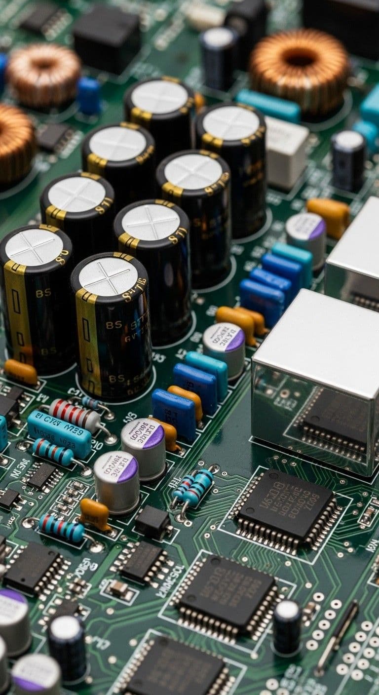
Copper weight and current paths
Heavier copper suits power and thermal routes but consumes more space.
- Maximum current per trace
- Voltage drop on long routes
- Solderability limits for thick copper
Layer count and signal planning
More layers often reduce noise but increase fabrication cost.
- Analog and digital ground separation
- Power plane planning
- Controlled impedance when required
Fabrication notes
Clear notes on the job prevent misinterpretation at the fab.
- Drill type and tolerances
- Surface finish specification
- Dimensional constraints